90
9152BINDCO02/10
ATA8743
uses to increment (or decrement) its value. The Timer/Counter is inactive when no clock source
is selected. The output from the Clock Select logic is referred to as the timer clock (clk
T0
).
The double buffered Output Compare Registers (OCR0A and OCR0B) is compared with the
Timer/Counter value at all times. The result of the compare can be used by the Waveform Gen-
erator to generate a PWM or variable frequency output on the Output Compare pins (OC0A and
OC0B). See
Output Compare Unit
on page 91 for details. The Compare Match event will also
set the Compare Flag (OCF0A or OCF0B) which can be used to generate an Output Compare
interrupt request.
20.2.2
Definitions
Many register and bit references in this section are written in general form. A lower case
n
replaces the Timer/Counter number, in this case 0. A lower case
x
replaces the Output Com-
pare Unit, in this case Compare Unit A or Compare Unit B. However, when using the register or
bit defines in a program, the precise form must be used, i.e., TCNT0 for accessing
Timer/Counter0 counter value and so on.
The definitions in Table 20-1 on page 90 are also used extensively throughout the document.
Table 20-1. Definitions
20.3 Timer/Counter Clock Sources
The Timer/Counter can be clocked by an internal or an external clock source. The clock source
is selected by the Clock Select logic which is controlled by the Clock Select (CS02:0) bits
located in the Timer/Counter Control Register (TCCR0B). For details on clock sources and pres-
caler, see
Timer/Counter Prescaler
on page 136.
20.4 Counter Unit
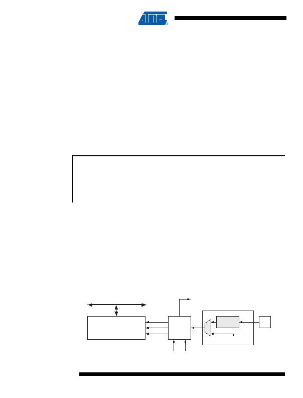
The main part of the 8-bit Timer/Counter is the programmable bi-directional counter unit. Figure
20-2 on page 90 shows a block diagram of the counter and its surroundings.
Figure 20-2. Counter Unit Block Diagram
BOTTOM The counter reaches the BOTTOM when it becomes 0x00.
MAX
The counter reaches its MAXimum when it becomes 0xFF (decimal 255).
TOP
The counter reaches the TOP when it becomes equal to the highest value in the
count sequence. The TOP value can be assigned to be the fixed value 0xFF
(MAX) or the value stored in the OCR0A Register. The assignment is depen-
dent on the mode of operation.
DATA BUS
TCNTn
Control Logic
count
TOVn
(Int.Req.)
Clock Select
top
Tn
Edge
Detector
( From Prescaler )
clk
Tn
bottom
direction
clear
发布紧急采购,3分钟左右您将得到回复。
相关PDF资料
ATAVRRZ200
KIT DEMO AT86RF230
AV101-12LF
ATTENUATOR HIP3 0.70-1GHZ 8-SOIC
AV102-12LF
ATTENUATOR HIP3 1.7-2GHZ 8SOIC
AV113-12LF
ATTENUATOR HIP3 2.1-2.3GHZ 8SOIC
AXUV100G
SENSOR ELECTRON DETECTION
B0205F50200AHF
XFRMR BALUN RF 200-500MHZ 1608
B0310J50100AHF
XFRMR BALUN RF 300-1000MHZ 0805
B0322J5050AHF
XFRMR BALUN RF 300-2200MHZ 0805
相关代理商/技术参数
ATAB5275
功能描述:射频开发工具 LF Tx Antenna driver board (TPMS) RoHS:否 制造商:Taiyo Yuden 产品:Wireless Modules 类型:Wireless Audio 工具用于评估:WYSAAVDX7 频率: 工作电源电压:3.4 V to 5.5 V
ATAB5276
功能描述:射频开发工具 1A Antenna Driver Demoboard RoHS:否 制造商:Taiyo Yuden 产品:Wireless Modules 类型:Wireless Audio 工具用于评估:WYSAAVDX7 频率: 工作电源电压:3.4 V to 5.5 V
ATAB5278
功能描述:射频开发工具 LF Tx Antenna driver board (PEG) RoHS:否 制造商:Taiyo Yuden 产品:Wireless Modules 类型:Wireless Audio 工具用于评估:WYSAAVDX7 频率: 工作电源电压:3.4 V to 5.5 V
ATAB5279
功能描述:射频开发工具 LF Transmitter with ATA5279 RoHS:否 制造商:Taiyo Yuden 产品:Wireless Modules 类型:Wireless Audio 工具用于评估:WYSAAVDX7 频率: 工作电源电压:3.4 V to 5.5 V
ATAB5282
功能描述:BOARD EVAL LF 125KHZ ANT DVR 3CH RoHS:是 类别:RF/IF 和 RFID >> RFID 评估和开发套件及电路板 系列:Smart RF 产品培训模块:M24LR64 Dual Interface EEPROM 标准包装:1 系列:- 类型:读取器模块 频率:13.56MHz 适用于相关产品:M24LR-64-R 已供物品:2 根基准天线,I2C 和 RFID 读取器,样品 其它名称:497-10480
ATAB5283
功能描述:射频开发工具 LF Rx Board 1 channel (TPMS)
RoHS:否 制造商:Taiyo Yuden 产品:Wireless Modules 类型:Wireless Audio 工具用于评估:WYSAAVDX7 频率: 工作电源电压:3.4 V to 5.5 V
ATAB5423-3-B
功能描述:射频开发工具 UHF Transceiver Base station Board 315MHz
RoHS:否 制造商:Taiyo Yuden 产品:Wireless Modules 类型:Wireless Audio 工具用于评估:WYSAAVDX7 频率: 工作电源电压:3.4 V to 5.5 V
ATAB5423-3-WB
功能描述:射频开发工具 UHF TRx Application Board 315MHz RoHS:否 制造商:Taiyo Yuden 产品:Wireless Modules 类型:Wireless Audio 工具用于评估:WYSAAVDX7 频率: 工作电源电压:3.4 V to 5.5 V